

Introduction: JVSCab2PC - SEGA JVS Cabinet to PC I/O Replacement Board


After years of honoured service, the NAOMI motherboard in my Crazy Taxi arcade cabinet died and I had to run for cover.
I am used at pre-90's Arcade cabinets conversions and have already developed some interface board for the task (e.g. THIS and THAT instructable), but this was the first time I had to face a JVS cabinet convertion.
To make a long story short, the main "complexity" in such a convertion lies in the control panel interface board, also known as input-output board (I/O board in the following). Despite a genuine JVS I/O board hosts a USB connector, it would not work if directly connected to a PC. This is because JVS calls for RS485 communication, which is different from USB.
Here lies the main "problem" to solve in order to have a cabinet from the JVS era comunicate with a PC: convert that not-PC-friendly signal into something a PC can understand and handle.
Protocol conversion/manipulation is not my piece of cake, but I have some experience with arduino and PCB design, so my solution was to completely remove the native JVS I/O board (nowsecurely stored in a crate, close to that of the lost Ark :) ) and lay down my own device.
In this instructables I will (briefly) introduce you to the genuine SEGA I/O board hardware and the possible approaches to interface cabinets from the JVS era to any PC. I will describe the hardware and software I developed for the task, its features and how to install it. I will also share all the files to have the interface PCB I layed down readily manufactured at JLCPCB (affiliated link).
Please notice that the board here described is used to connect the control panel of a genuine JVS cabinet to a PC. It allows to play software emulated games on a genuine cabinet. It cannot be used to connect a general PC peripheral (wheel, joypad, keyboard, etc etc) to a NAOMI motherboard or any other JVS platform.
Step 1: SEGA JVS I/O Board: an Overview


Starting from the latest 90's many manufacturers adopted a very specific standard for the harness of their cabinets called Jamma Video Standard (JVS). This standard was intended to be the evolution of the previous, mid 80's jamma standard.
The single 56 pin "JAMMA" connector where all signals (audio, video, inputs) converged was abandoned (even if still supported in jamma kits) in favour of a series of separate connectors (HD-15/VGA for video, RCA jacks for stereo audio) and a serial comunicaton protocol for controls.
The I/O board is in charge to monitor player inputs and send them to the main board via RS485. It also routes outputs from the mainboard to cabinet's lamps and actuators.
In the following a brief description of I/O boards you could find in SEGA cabinets from the JVS era. Please notice that a good number of different I/O boards where developed by manufacturers that adopted the JVS standard for their cabinets/games (Capcom, Taito, NAMCO, Konami, SEGA). Here we will deal with SEGA I/O boards only.
SEGA JVS I/O Board Hardware
SEGA revisited it's board various times during the years from NAOMI to Lindberg arcade game platforms production, with three main revisions.
The first version of SEGA JVS I/O board (also known as "Type 1") was labelled 837-13551-92 (see attached picture). This has a big Toshiba microcontroller (TMP90PH44N-8604 @15MHz) in charge to monitor control panel inputs (both analog and digital) and send them to the main board. All digital inputs are optoisolated (8x NEC PS2801-4 photocouplers) and connected to dedicated pins in the microcontroller.
Another function of the I/O board is to handle outputs informations incoming from the game board and route them to cabinet lamps and actuators. The microcontroller can output currents of only few mA, so a parallel of dual high power MOSFETs (4x Motorola 5850) in series to a bus buffer (VHC240) comes to the rescue to drive outputs loads.
The second revision of the board (SEGA JVS I/O 837-13844-02) separated inputs and outputs adopting a 40 pin connector for inputs (up to 12 for player) and a 34 pin dedicated connector for up to 22 outputs. This version is rarely seen and features the less compatiblity with games.
The third revision (SEGA JVS I/O 837-14572) is very similar to the first version, with the 60 pin connector back in place to host digital inputs and outputs (same pinout as version 1) and an additional 20 pin connector for up to 20 additional outputs, for a total of 28 outputs. This board is full-SMD, with all components (cleanly) layed on the same side of the board.
Detailed pinout of all three main revisions >>HERE<<.
Step 2: The Approach

Digging the web, the most commonly adopted reasonable* (trademark :D) strategies to interface a JVS cab to a PC are based on the convertion of the JVS RS485 signal to RS232 through an intermediate hardware (converter) placed between the I/O board output and the PC. A HID emulating software ends the chain.
The "input path" of such solution is "control panel inputs -> JVS I/O board -> RS485 to RS232 converter -> HID emulating software -> platform emulator".
Most of the time those hardwares show the limit of not supporting analog inputs, which was essential for me (remember? I have a NAOMI Crazy Taxi cabinet to put back on track).
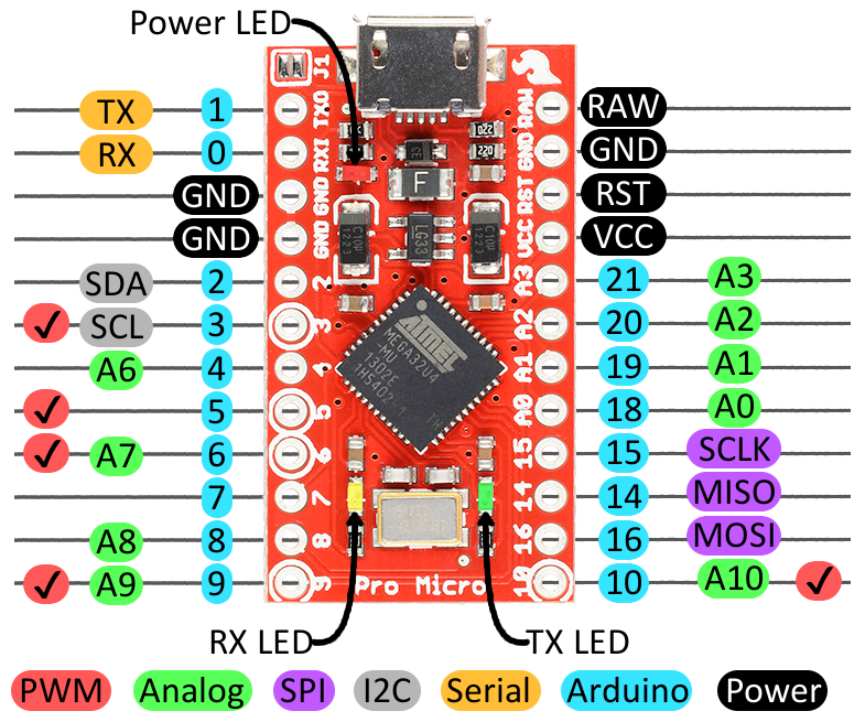
It was a no-brainer to remove the JVS I/O board all toghether and replace it with a dedicated input board built around a microcontroller capable of natively emulate a HID USB peripheral. Yes, the usual ATmega32U4 arduino we are all familiar with comes handy in these situations.
The path reduces to "control panel input -> HID board -> platform emulator".
Main features of this approach are:
- Multi HID emulation (keyboard, joystick, mouse) made simple (thanks to Arduino/Community libraries)
- Analog inputs support
- Multiplatform (Win, Linux, Mac)
- Open source software
- Easily expandable/improvable firmware without a dedicated programmer (thanks to Arduino IDE)
*When I say "reasonable" I mean "something that don't ask for cutting wires" (and with a limited complexity, if possible): Our cabinets are valued from both a hystorical and economical point of view and, today more than yesterday, preserving them as conceived by manufacturers is mandatory.
Step 3: JVSCab2PC Hardware

Here follows a description of the JVSCab2PC hardware.
A/D INPUTS
Genuine SEGA JVS I/O boards handles a total of 14 inputs per player (start button, coin switch, 4 joystick directions, 7 buttons and player service button), 2 auxiliary switches (test and tilt) and 8 analog inputs.
Being the Arduino pro-micro's number of GPIO pins not sufficient to handle all those inputs, I used four 8-bit input shift registers. Control panel (parallel) digital inputs are "serialized" by registers and sent via SPI to the arduino which, in turn, emulates a user definable HID.
All eight analog inputs are directly wired to Arduino pro-micro analog pins so no additional hardware is required.
OUTPUTS
Outputs are multiplexed via an output shift register (74HC595). A simple built-in driver circuit made of a NPN series Darlinghton transistors (ULN2003) drives cabinet lamps. Each transistor is capable of outputting a maximum of 500 mA of continuous current (1A total over all seven outs!!), which is enought for those 1W filament bulbs used in view/start lamps.
!! Warning !! Driving loads such as a force feedback motor would call for an adeguate, high current, external driver board. Do not attempt to drive loads with a current consumption higher than 500 mA from the on-board driver circuit or you will kill the board.
I preferred to leave coin counters unwired because an incorrect wiring could potentially kill the I/O board. Maybe in a next revision, but do not count on it too much :)
I/O CONNECTORS
As we have seen in STEP 1, SEGA released three different JVS I/O board versions, with different pinouts. This project, even if built around rev.1, hosts additional connectors in order to be compatible also with rev.2 and 3.
Here follows the list of connectors present on-board:
CN1 - 34 pin connector for outputs (type 2 board, unpopulated in pictures)
CN2 - 40 pin connector for digital inputs (type 2 board, unpopulated in pictures)
CN3 - 60 pin connector for digital inputs and outputs (type 1 and 3 boards)
CN4 - 26 pin connector for analog inputs (type 1,2 and 3 boards)
Inputs and outputs from different connectors are hardwired toghether. Especially for inputs, this has the welcome collateral effect of giving the user direct access to all inputs. In the case of cabinets with a considerable number of unused input pins, this makes possible to wire additional buttons for, in example, front end menu navigation.
Disclaimer: this is NOT an invitation to drill your cabinet control panel to host extra buttons! Preserving the originality of our beloved arcade machines for future generations of enthusiasts is a social duty.
An additional connector (CN7) hosts three PWM and three digital pins for future I/O applications. Two remarcable examples of such applications could be force feedback support (not so easy implementation), or support for optical peripherals (e.g. spinner, trackball).
!! Warning !! CN7 pins are directly connected to arduino GPIOs so are not capable of driving loads! If used as outputs, you must connect an adeguately dimensioned driver board between these pins and the load to drive.
POWER SUPPLY
All I/O board IC's are directly powered by USB connector. The built-in output driver circuit calls instead for an external source of +5V. Connector CN5 (or CN6) has to be used to supply external power (+5V, 1.5A minimum). This most likely will be the original PSU already mounted in the cabinet.
Please notice that JVSCab2PC board is NOT protected against inverse polarization. By supplying power with reverse polarity to CN5 (or CN6) you will 100% fry all the components, microcontroller included. In the unfortunate situation where the I/O board is already connected to a PC, you have a good chance of damaging that too.
Step 4: JVSCab2PC Sketches!
Having an open firmware makes the difference when dealing with a device that will potentially be used in cabinets with very different control panel characteristics. A two players SEGA NAOMI Universal cabinet, in example, has a whole lot of digital inputs and no analogs. On the other side, a Crazy Taxi / 18 Wheeler / Jambo Safari cab has a very limited number of digital inputs but three analog inputs. A closed, one-fits-all firmware would be forced to keep all differencies into consideration, which in turn would make the code verbose and difficult to optimize.
An open source firmware allows instead ad-hoc code optimizations. In this optics, I wrote two different DEMO sketches, for two, main cases. You can download them (and some useful utility sketch) >>HERE<< (Github).
Follows their description.
File name: JVSCab2PC_2P
Application: two players cabinet with up to seven buttons per player
Description: This sketch emulates a gamepad with 30 digital inputs and no analogs.
Control panel inputs: P1/P2 start, P1/P2 buttons (7 each), P1/P2 joysticks.
Service switches: P1/P2 service, Test, Tilt, P1/P2 coin.
Notes: Any control panel and/or service button press sends a fixed gamepad button press (0-29, not user definable). Digital inputs are software debounced.
File name: JVSCab2PC_DRIVING
Application: one player driving cabinet with sequential shifter
Description: This sketch emulates a gamepad with 3 analog axis and 12 digital switches.
Control panel digital inputs: P1 start, P1 coin, P1 up (wired as "Drive" in Crazy Taxi cabinet ), P1 down (wired as "Reverse" in Crazy Taxi cabinet).
Service switches: P1 service, Test.
Analog Axes: Steer, accelerator, brake.
Notes: Registers handling is kept verbose to help figure out how it works. Digital inputs are software debounced. Shift function is coded. If "start" button is held pressed, any other button will send a new/alternate button press. This function is especially useful in cabinets with a limited number of inputs.
Common to sketches:
All make use of the brilliant Mattew Heironimus joystick library, which shines in arcade applications. This library is compatible with keyboard and mouse libraries, so user can turn JVSCab2PC into a multi-HID device.
Inputs state changes are serialized by input shift registers and monitored at any loop cycle. When the input state changes, button press/release is sent to the PC via USB. Input shift register code is based on THIS article by Nick Gammon.
At the moment, sketches do not handle outputs, even if the I/O board object of this instructable actually has a built-in driver for low wattage loads. If you want to test a simple output routine alternatively actuating outs 3 by 3 at a frequency of 1Hz, simply add at the bottom of the sketch the following function:
//outputs variables
unsigned long blinkTime;
bool oflag;
byte obyte;

void OutRegHandle(){
//button lamps alternating flashing. Start button lamp mask 0b00001000 (OUT1_1, pin 51 on CN3)
//hardware outputs array: OUT1_3 | OUT2_3 | OUT1_2 | OUT2_2 | OUT1_1 | OUT2_1 | NC | NC
  if(millis()-blinkTime > 500) {
    blinkTime = millis();
    oflag = !oflag;
    if(oflag == 1){
      obyte = 0b10101010;
    }
    else{
      obyte = 0b01010101;
    }
    SPI.transfer(obyte/*, sizeof(obyte)*/);
    digitalWrite (outRegPin, LOW);
    digitalWrite (outRegPin, HIGH);
  }
 }
Call "OutRegHandle()" function in the main loop, upload the new sketch to your JVSCab2PC board and your outs will start blinking as if it were Christmas :)
Warning: activate outputs at your own risk! The built-in driver board can deliver up to 500 mA on a single channel (1A total on all seven outs!). In case of an excessive load the driver board will be likely damaged.
Step 5: JVSCab2PC I/O Board Input Lag?

Measuring a device input lag is a very serious matter, as demonstrated by efforts some integralist gamer and talented programmer put in to shed light on the subject :)
Unfortunately, I have not the hardware by hand at the moment for an "accurate" measurement, nor I am motivated enought to spend a good amount of money in a device I would use once*.
So, I limited myself in giving an estimate of the input lag induced by the code itself, measuring the time it takes to complete a code loop when 6 switches are actuated simultaneously (see attached picture for test setup).
Here are the results:
JVSCab2PC_2P: 3.8 - 5.0 ms (with an "idle" loop time < 0.4 ms)
JVSCab2PC_DRIVING: 8.6 - 9.8 ms (with an "idle" loop time < 3.2 ms)
By comparing the two, we can see that introducing analog controls handling instructions adds a not negligible load to the cycle. It's worth noting, anyway, that racing games do not ask for strict timings like, in example, fighting games.
Please notice that pressing 6 buttons simultaneously (which in this specific case means "in the exact same code loop cycle") during gameplay is a extreme condition, potentially possible in a 2 players cabinet, but not possible in a racing cabinet. If we measure lag when pressing 3 buttons (again: in the exact same code loop cycle) those values reduce to:
JVSCab2PC_2P: 1.0 - 1.6 ms
JVSCab2PC_DRIVING: 4.8 - 6.0 ms
A single buttonpress reduces lag at idle loop time levels.
To these values we should add a coefficient given by polling rate implications and then we would have an estimate of the I/O board lag (controller lag). To compute the whole SYSTEM input lag you should add game engine lag and display lag, but these are not caused by the I/O board.
*Sooner or later I will buy an Arduino USB shield and I promise myself to update the present instructable with results.
Step 6: Hardware Installation (SEGA NAOMI)


I only own a Crazy Taxi*, so I will describe how to install the JVSCab2PC board in that cabinet. The procedure is the same for any cabinet on SEGA Universal base, anyway.
To gain access to the SEGA NAOMI I/O board, follow these steps:
- open the control panel by removing the three M8 tamperproof screws that lock it
- remove the metal plate that locks the front panel (2xM4)
- remove two M4 side screws placed on the leftmost and rightmost extremes of the horizontal part of the front panel
- slide out screws caps and remove the 4xM6 tamperproof screws underneath
Now you have full access to the NAOMI I/O board (under a mess of cables). Remove it by unscrewing the 4 screws that keep it in place, and install JVSCab2PC.
Connect the big 60 pin connector (digital inputs/outputs) and the 2 pin connector (analog inputs) respecting their orientations. The notch must face the internal of the board in both connectors. Refer to serigraphs in case of doubt.
If you plan to use outputs, connect the +5V external power source to CN5 (or CN6, they are in parallel).
Please, be careful in connector insertion phase!! Pay maximum attention to the orientation of connectors, in particular CN5 (or CN6). Here power to the output driver circuit is fed. The circuit is NOT protected against inverse polarization so, if you connect it reversed, the I/O board will be damaged (and potentially the PC too, if already connected!!).
Connect JVSCab2PC with a USB connector to one of your PC's USB ports.
You may well be asked to install drivers for JVSCab2PC (and it will happen every time you change USB port). Follow THIS guide for Arduino driver installation.
JVSCab2PC has the same dimensions of a genuine SEGA JVS I/O board. I tried to keep as much as possible the general layout similar to that of a SEGA JVS type 1 I/O board, just to make the installation easier.
You can now test your JVSCab2PC with any gamepad test software, being it online or installed in your PC. I have uploaded a simple batch file to evoke windows 7 joypad tester utility >>HERE<< (Github).
At this point you only have to set up the board in your game platform emulator (and front end) as you would with a common gamepad. This procedure is different from emulator to emulator, so it will not be covered here.
*yes, my poor Crazy Taxi cabinet has seen better days. Nevertheless I do my best to keep it up and running ;)
Step 7: Does It Work??


Yes, it works!
Attached a raw video showing JVSCab2PC installed in my Crazy Taxi.
You can see both inputs and outputs in action.
I am sorry: videomaking is not my piece of cake, nor I am the best Crazi Taxi player out there :P
Step 8: SMD Tips and Tricks
This project uses surface mount devices (SMD) and I opted for JLCPCB SMT assembly service because I had succesfully used their service in a previous project and was very happy about the results.
Dealing with SMDs is inevitably more articulated than with through hole parts (you have to upload not only your zipped Gerber files, but also BOM and CPL files, select the components between those available in the Manufacturer catalogue and make some accurate visual checking before being done), but with the help of THESE instructions and JLCPCB online submission form everything went smooth and well.
I took some notes about the "criticalities" I found during my (limited in number) experiences with SMD assembly. I also noted solutions, for future use:
- Triple check your design before submission, by running your software design rule check (DRC) and electrical rule check (ERC). It will be difficult to fix those after the realization.
- If you are running on an old PCB design software version, use the correct exporter file for CPL and BOM files. I had to use "jlcpcb_smta_exporter_v7.ulp" instead of "jlcpcb_smta_exporter.ulp" because the latest was not compatible with my board design software version (old).
- Parts without a value could be left out by the ULP, depending on your choice. Be sure to uncheck "skip parts with missing values" if present.
- Check any single component to be sure it will fit on the board. It happened to me, in example, that a resistor array was misinterpreted as a regular resitor. You will spot such an error immediately if you take a look at components.
- After the Gerber, BOM and CPL files are uploaded, a representation of the board will be displayed for a first components population check. It is possible that some IC has the wrong orientation and is completely misplaced at this time. No problem!JLCPCB engineers review and take care of components positions and orientations for you before the assembly! Continue with your order: they will contact you before assembly if criticalities in components placement and orientation are present.
- The board representation screen is a good place to check for missing components (see also point #2 of this list). Carefully go though all the board, be sure that all components are there (no matter their exact position and orientation, as said) and go back if something is missing.
- Components selection is the most important (and funniest, in my opinion) phase. If the automatic selected part is not available or in inventory shortage, do not desperate! Use a more generic term in the part research field. In example: use 74HC14 instead of CD74HC14M and more options will be in your hands.
- When you are done with components selection, save your components list in the shopping chart. This is because it could be the case you want to make some modification to your design after that, and uploading a newly generated BOM will force you to check/select components once again. The shopping chart components list is saved in BOM format, so it will be a matter of uploading that to have all previously selected components directly listed.
Throughout the entire assembly planning process of your device, you never have the feeling of being left alone... proceed with caution and trust and it will all be fine :)
Step 9: Acknowledgments


PCB manufacturing and SMT assembly of this project was sponsored by JLCPCB, a high-tech manufacturer specialized in the production of high-reliable and cost-effective PCBs.
Their customer service is fast and helpful and PCBs a great value for your money!
By registering at JLCPCB via THIS LINK (affiliated link) you will receive a set of coupons for your orders. Registering costs nothing, so it could be a nice way to give their service a due try ;)
Gerbers, BOM and CPL files to have JVSCab2PC manufactured are available >>HERE<< (Github). BOM files already contains adeguate components from JLCPCB parts catalogue.
My projects are free and for everybody. You are anyway welcome if you want to donate some change to help me cover components costs and encourage the development of new projects.
>>HERE<< is my paypal donation page, just in case you want to push the development of new projects ;)


![Tim's Mechanical Spider Leg [LU9685-20CU]](https://content.instructables.com/FFB/5R4I/LVKZ6G6R/FFB5R4ILVKZ6G6R.png?auto=webp&crop=1.2%3A1&frame=1&width=306)


