
Summary of Contents for Spectravideo SVI 318
- Page 1 SERVICE & TECHNICAL MANUAL [VOL.1 l SVI318/328 {MKI/MKII) COMPUTER SYSTEM SPECTRAVIDEO...
-
Page 3: General Description
- ce r t i f ie d p e r iphe r a l s is l ik e ly to r e s u l t in i n t e r f e r e nce t o ra d i o a n d TV rece p t i on . (SVI) SPECTRAVIDEO INTERNATIONAL LTD., HONG KONG F i r s t E d i t i on... -
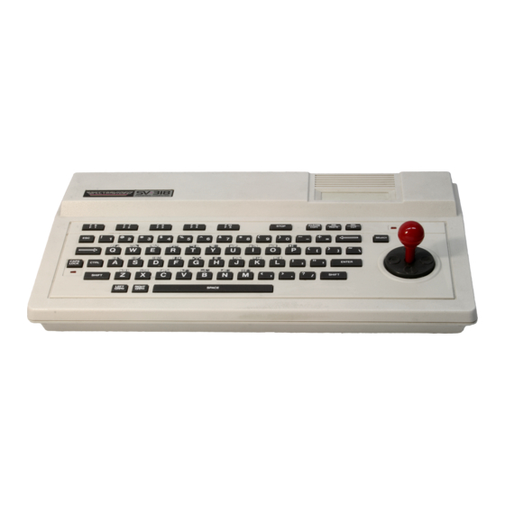
Page 4: Operator Interface
CHARACTERISTICS T he fo l l ow i ng l i s t s the cha rac ter i s t i c s o f and acce s s o r i e s for SVI-3 1 8 / SVI-3 2 8 home compu t e r . -
Page 5: Power Indicator
POWER INDICATOR is an LED that monitors the power indicator supply. When on, SVI-318/SVI-328 I I . indicates the presence of power to and Mark... -
Page 6: System Introduction
SYSTEM INTRODUCTION This manual is arr anged in the following sections: and Mark 11 personal General information about the SVI-318/SVI-328 computer and its peripherals, including model humber and feature kit descriptions. Information on how to remove and replace the major assemblies that make up the computer. - Page 7 Remove seven retaining screens. Remove the cover.
- Page 8 Remove the screens on the metal cover. Remove the metal cover. 2 . 3...
- Page 9 To r e-a s s e mble, u se th e above pro ce dure s in the rever se order.
- Page 10 d hark SVI-318/SVI-328 II EXPANDER BUS SIGNAL DESCRITPION I / 0 : DESC RI PTION : NAME : + 5V powe r supp l y . 300mA cur r e n t i s av a i l a b l e f o r a l l p e r iphe r a l c a rd s.
- Page 11 PIN: NAME: I/0: EXCSR Th i s is the ex te rn a l CPU - f rom-VDP READ se l ec t s ignal , an d i s use d b y S pec t ravideo g ame adaptor for cole c oyM games.
- Page 12 PIN: NAME: DESCRIPTION: Buffered MEMORY BANK CONTROL signal. Pulling t h i s signal LOW enables the b nk 32 p or ti on of the memory (32K, Addr.-- 8000H-FFFFH), disables the user RAM on board through sig nal . Buffered MEMORY BANK CONTROL signal.
- Page 16 DIAGNOSTIC TEST AND TROUBLE SHOOTING CHART A cartridge is available to test computer hardware: the SVI-318/SVI-328 CPU and OUTPUT BUFFERS to the EXPANDER USER RAM VIDEO RAM (VRAM) P ROGRAMMABLE SOUND GENERATOR (PSG) SOUND CHANNEL VDP INTERRUPT CAS SETTE LINE (CASW/CASR, ME/RE) �...
-
Page 17: Data Write
XXXX ADDRES S: address the memory l oca t ion a t wh ich an error is found. da ta wr itten to the loca t ion addres se d by DATA WRITE: the ab ove address . da ta read from the l oca t i on addre s se d by DATA W R ITE: the above address . - Page 19 SA200 MAINTENANCE EQUIPMENT A l i g nme n t D i s k e t t e T he SA12 4 a l i gnme n t d i s k et t e i s u s e d for alignment of the SA200 . The f o l l ow ing a d j u s t me n t s and ch e c k s c an be ma d e u s ing the SA12 4 .
- Page 20 " S o f t E r r or" De tect i on and Cor re c t ion Sof t err o rs are usua l l y cause d by: Airb or ne contam inan ts t ha t pass be tween the rea d/w r i te head and t he d isk . Usua l l y, t hese contam i nan ts can be remove d by t he ca r t r i dge se l f- c lea n i ng wipe r.
- Page 21 Seek E r ro r Stepper ma lf unction Car riage b i nds . To recove r f rom a seek e r ro r , reca l i b rate to t ra ck a nd perform anothe r I .
- Page 22 ELECTRICAL/FUNCTIONAL Co nnec t t h e powe r s u pp l y and modu l a t o r t o the compu t e r and the TV rec e ive r ( se l ec t t h e r i gh t c ha n nel and the TV- Sy s t em ) . Turn on the lowe r sw i t c h , the "POWER ON"...
- Page 23 amme 1 0. Pre ss "F4" and observe the progr conte nt is l i sted out . 1 1 . Type "NEW" and pre s s s "ENTER", t.he pre s s "F4" aga in to con f i rm the am;;...
- Page 24 Thr e e c r o s s -ma rked co l o u r cu r s o r s shou l d be app e a r e d on t h e TV sc r e e n . Connec t t h e j oy s t i c k to s o c k e t �onne c t o r 1 i n the r i gh t han d s id e o f t he un i t .
- Page 25 Type "CLOAD " BAR'"' and re s s " ENTER" 1 4 . P re s s t h e "P L.AY" b u t t o n on the �a s s e t t e a f t e r the " FOU ND : BAR" and ' OK' a p pe a re d on t he s c r e en .
- Page 26 1 0 . Type t he f o l l ow i ng p ro g ramme : 1 0 SCREEN 1 20 C I RCLE ( 1 2 8 , 96 ) , 8 0 , 1 1 30 PAINT ( 1 2 8 , 96 ) , 1 1 40 GOTO 40 ( P r e s s "...
- Page 27 Typ e "D I R" and "ENTE R" , t h e direc t o r y l i s t shou l d be app e a r e d press on t he . s c r e en . "DDT"...
- Page 28 Tll OUB LE SB001'IRG CHAR T POS S I BL E CAUSE SYMPTON REMEDY T u rn on pow e r sw i tc h wh ich i s N o pow e r Pow e r s w i tch not on r i g h t -han d s i d e o f the t u rne d on mac h i ne .
- Page 31 10 REM Memory bank ram s i z e t e st p rogram Ma k e su re you ha ve 64K ram ca rd 20 REM One ha ve BK2 1 on , t he o ther ha ve BK31 on , 30 REM ( i n 32K op t i on )
- Page 32 LD ( BK2 1 ) , HL SAVE RAM SIZE 5 1 0 DATA 2 2 , 42 , DO :REM ORG BANK COND 5 2 0 DATA 7 8 : REM LD A , B· 530 DATA D3 , 8C :REM ( 8 CH ) , A 540 DATA FB...
- Page 33 S CREEN 1 FOR I=O TO 2 0 CIRCLE ( 1 2 8 , 96 ) , I*5 NEXT I LINE ( 0 , 0 ) - ( 2 5 5 , 1 9 1 ) , , B L I N E ( 0 , 0 ) - ( 2 5 5 , 1 9 1 ) ; L I N E ( 2 5 5 , 0 ) - ( 0 , 1 9 1 ) - che ck &...
-
Page 34: System Architecture
TIIEOR Y OF OPERATION DESCRIPTIOR SYSTEM ARCHITECTURE T he Spe c t rav ideo SVI-3 1 8 / SVI-328 and MarK II home compu t er is a compu tat ional tool ba s e d on a Z i log BOA microcomputer system F igure 4-1. The Zilog 80A microproces sor uni t ( �... - Page 35 3.58MHZ Joystick Fire llutta1 MEI.fJFCi BANK FIRE l3I.1I'ltN Plld dl.e * SIT-328 DATA BUS INTERFACE +SV - GND- C1. 0C K - REGISTER ARRAY Cl!tU TIMING ADDRESS LOGIC AND I CPU BUFFERS AND CPU ,.-&IT SYSTEM$ INPUTS ADDRRUBUS CONTROL CONTROL OUTPUTS Z80CPU Block Diagram FIG.4-2...
-
Page 36: Special Purpos E Registers
CPU RESGISTERS T he Z-80 CPU �o n t a i n s 20 8 b i t s o f R /W memory tha t a re ac c e s s a b l e to the p rog ramme r . F i gu re i l l us t ra tes how th i s me mory is con f i gu r e d i n t o e i gh t e e n 8-b i t re g t e r s an d fou r 1 6-b i t r e g i s t e r s . - Page 37 MEMORY INTERRUPT REFRESH VECTOR INDEX R E G I S T E R IX I N DEX R E G I S T E R IY STACK POINTER S P P ROGRANHE C OUNTER P C Z-80 CPU REGI STER CONFIGURATION F ig.
-
Page 38: General Purpose Registers
Memory Re f r e sh Reg st e r ( 5 ) Z-80 CPU conta i n s a me mory re f tesh counte r to ena b l e dynamic memories used w th the s ame e a s e as s t a t i c memori es. S e ven b i t s of t his 8-b i t reg i s t e r are a u toma t i c a l l y inc remente d after each i n s t r u c t ion f e tch. -
Page 39: Cpu Control
LOGIC UNIT (ALU) The 8-b i t a r i t hme t i c. and l o g i c a l in s t r uc t ion of the CPU are execu t e d in the ALU. - Page 40 Ins t ruct ion Set T he Z80 m i c rop roce s s or h a s o ne o f t he mo s t pow e r f u l and ve r s a t i l e in s t r uc t i on se t s �va i l a b l e in any 8-b i t m i c r o p roce s s o r .
- Page 67 Symbo l ic Notation Symbo l Operat ion M S B of the r e s u l t is 1 . S i g n f l a g . i f t he Z e ro f l a g . 1 i f t he r e su o f t he o p e r a t i on i s...
- Page 68 Any 1 6-b i t l o ca t i o n f o r a l l the add re s s ing modes a l l owe d f o r t h a t i n s t ru c t i on . Any one o f the two index reg i s t e r s IX o r IY .
- Page 69 S V I -3 1 8 AND S V I -3 2 8 I / 0 PORT LOCAT I ON REMARK I / 0 PORT R /W DESCR I PT I ON PR INTER WR I T E DATA P ORT l OH P R I NTER DATA S TROBE...
-
Page 70: Pin Descriptions
P IN DESCRIPTIONS ac t i v e H i gh , 3 - e ) . Add re s s Bus ( ou tp u t , A0- A15 form a 1 6 -b i t a dd r e s s b u s . The A dd r e s s Bus p r o v i d e s a dd r e s s f o r t he... - Page 71 Mach ine Cyc l e One ( output , act ive Low) . MREQ , indicates that tbe cur rent mach i ne c � l e i s the opcode fetch cyc l e of an inst ruct i on execut ion . Ml , together with cyc l e .
- Page 72 VIDEO DISPLAY PROCESSOR TMS- · 9918A OR 992.9 · TM S - 99 1 8 A or 9929 P gene r a t e s a l l con t r o l , s ync h ro n i z a t i o n and compos i t e v i d eo s i g na l s .
- Page 73 S p r i t e P l a n e s a re u s e d f o r t h e 3 2 s p r i t e s in t h e Mu l t i c o l o u r a n d Gra p h i c s mod es .
- Page 75 EXTV I D E x t e r n a l v i d e o i n p u t u s e d . N T S C c o l o u r b u r s t f re q u e n c y c l o c k .
- Page 77 B LACK .311 EXTE R N A L BACK D R O P CSO L I O COLOR I V I D E O INPUT PATT E R NS ICHARACTE R · O R I E N T E O J --...
- Page 78 SVI -3 1 8 / SVI-3 2 8 AND MARK I I RAM/ROM DES C R I PT ION T he S V I - 3 1 8 / S V I - 3 2 8 and �la r k I I ba s i c un i t ha s 3 2 K ( S OK ) * b y t e s o f R a n d om A c c e s s t·1 emo r y ( RAl-1) d i v i d e d i n t o two g r o u p .
- Page 79 �!EMORY ( 41 1 6 ) 1 6384 1 BIT DYNAMIC MOS RANDOM ACCESS RAM . The 4 1 1 6 i s a 1 63 8 4 wo r d s b y 1 b i t Dy nam i c MOS I t i s d e s i gne d f o r mem o r y ap p l i c a t i o n s whe re ve r y l ow co s t and l a rg e b i t s t o r a g e a re impor t a n t de s i g n ob j e c t i v e s .
-
Page 80: Sound Generator
SOUND GeNERATOR PROGRAMMAB L E AY-3-89 1 0 T h e AY-3 -8 9 1 0 i s a r� g i s t e r o r i e n t e d sou n d g e n e r a t o r ( PS G ) . p r o g r a mm a b l e t h e P S G... - Page 81 b u s T o i n p u t da t a f rom I / O P o r t A to t h e CPU wou l d re qu i r e the fo l l ow i ng : La t c h a dd r e s s R7 ( s e l e c t E n a b l e re g i s t e r ) ' ' 0 "...
- Page 82 B u s D I Rec t i on , B u s Co n t ro l The s e b us c o n t ro·l s i g n3 l s a r e g e n e r a t e d d i r e c t l y by Z80A s e r i e s o f m i c r o p r o c e s s o r s t o c o n t r o l e x t e rna l and b u s op e ra t i o n s in the P S G .
- Page 83 The P ro grammab l e Soun d Gene r a t o r The P S G AY-3 -8 1 90 gene r a t e s a l l re qu i re d s o u n d un d e r s o f tware con t ro l . The r e a re t w o 8-b i t I / 0 p o r t s wh i ch a re p ro g r amme d a s fo l l ow : Prog ramm e d a s i n p u t po r t and i s u s e d f o r the i np u t s i gna l f rom two...
- Page 84 8255A THE PROGRAMMAB L E PERIPHERAL INTERFACE. The 8 2 5 5A PP I i s u s e d to s t robe the ke yboa r d l i n e s , t o int e r f a c e the j oy s t i c k f i re b u t t on sw i t c h , the p a dd l e and to cont ro l t h e ca s s e t t e tap e s y s t e m .
- Page 85 Re a d . " low'' o n t h i s input p i n enab l e s the 8 2 5 5A t o send the data or s t a t u s in f o rma t i o n t o t h e o n t h e d a t a bus .
- Page 86 The func t i on a l conf i g ura t i on o f e a c h po r t i s p ro g ramme d by t h e s y s t ems s o f t wa re .
- Page 87 mode ( i . e . , Whe n t h e r e s e t i n pu t g o e s " h i gh " a l l po r t s w i l l be se t t o t h e i np u t l l 2 4 l i n e s w i l l be i n t he h i gh i mp en d a n c e s t a t e ) .
- Page 88 8 2 5 5 P o r t A ( I nput P o r t ) P ad d l e o r Tab l e t Inpu t P a dd l e o r Tab l e t Input P a d d l e o r Tab l e t I nput P a dd l e o r Tab l e t I npu t T r i gg e r Sw i tch ( B u t t on ) o f J oy s t ick 1...
- Page 89 THE PROGRAMMAB L E COMMU N ICATION INTERFACE 8250-B INS8250-B FUNCTIONAL PIN DESCRIPTION The fo l l ow i n g d e s c r i b e s t h e func t i on of a l l INS8 2 50 i np u t / ou t p u t p i n s . S ome o f t h e s e d e s c r i p t i o n s re f e rence i n t e rn a l c i r c u i t s .
- Page 90 DLAB REG I STER Rece i ver Bu f f e r ( rea d ) , T ra n sm i t t e r H o l d i ng Reg i s t e r ( wr i t e ) I n t e r r upt E nab l e I n t e r r up t Iden t i f i ca t i on ( re a d on l y ) L i ne Con t ro l...
- Page 91 Da t a S e t Rea dy ( DSR ) , P in 3 7 : Whe n low , ind i ca t e s tha t the MODEM or data s e t i s re a dy t o e s t ab l i sh t h e commun i c a t ions l i nk and t r a n s f e r d a t a w i t h the T he DSR s i gna l i s MODEM-con t r o l func t i on input whose con d i t i on can INS8 2 50 .
- Page 92 Ou t p u t ( OUT 1 ) , P i n 3 4 : U s e r- d e s i g ne d o u t p u t t h a t can be s e t t o an act ive l o w p r o g r amm ing b i t 2 ( OUT 1 ) o f th e MODEM Con t r o l Reg i s t e r t o a h ig h leve l .
- Page 93 · th i s b i t spec i f i e s the numbe r o f �s top b i t s i n each t r a n sm i t t e d o r B i t 2 : r e c e i ve d s e r i a l cha r ac t e r .
- Page 94 die BS'ud Tab l es i l l us t rate the use of Rat e Gener tor with crysta l f re quencies of respect ive ly . For baud rates of 1 . 8432 MHz 3 . 0 7 2 MHz 38400 and be low the e r ror ob ta ined i s minima l .
- Page 97 D i v i s or U s e d t o P e r c e n t E r ror D i f f e re nc e between De s i re d & Act u a l De s i re d B a ud Ra te 1 6 x C l oc k G e n e r a t e...
- Page 98 P re s e n t E r ror D e s i r e d D i v i s o r U s e d to G e n e r a t o r Baud C l ock D i f f e re n t Be tween R a t e De s i r e d and Ac t u a l...
- Page 99 RS- 2 3 2 I n t e r f ace S p ec i f i c a t i o n C h a r a c t e r i s t i c s - E I A R S- 2 3 2 C S i g n a l R e c e i ve Mark...
- Page 100 MO DEM / CPU I n t er f a ce P i n As s i g nme n t s - [IA R S- 2 3 2 C P i n F u n c t i on P ro t e c t i v e G r o u n d T r a n sm i t te d D a ta ( D a t a O u t ) R e c e i v e d D a t a...
- Page 101 6845 CRT CONTROLLER SYSTEM BLOCK D I AGRAM D E S C R I P T ION As shown in STM-00 2 - I , t h e p r i ma r y func t i o n of the CRTC is to gene r a t e r e f r e s h ( MAO-MA 1 3 ) , ( RAO--RA4 ) , ( HSYNC ,...
- Page 102 C R T C D E S C R I P T I ON ( F i gu re S TM- 00 1 - I : B l ock D ia g r am ) C R T C c o n s i s t s o f p ro g rammab l e ho r i z on t a l a n d ve r t i c a l t i m i ng gene r a t o r s , T h e C RT C p r o g ramma b l e l i n e a r add re s s re g i s t e r , p ro g rammab l e c u r s o r l o g i c , l i ght pen ca p t u re r e g i s t e r , and c o n t ro l c i r c u i t r y for in t e r face t o a p r o c e s s o r bus .
- Page 103 REG I STER F ILE DESCRIPTION ( S ee Tab le 2 ) N ineteen reg i s t e r s in the CRTC can be acce s s e d by means of the data bus . Reg i s t e r a ddress ing and l engths a re shown in Tab le 2 . Add re ss Reg ister The Add re s s Reg i s ter is a 5-b i t write-on ly reg i s t e r use d as an "...
- Page 104 VERT ICAL TIM ING REG ISTE� R'4 , R5 , R6 , R 7 , R8 and R9 The po i n t of re f er e nce f o r ve r t i c a l re g i s t e r s is the top cha r ac t e r pos i t i o n d i sp l a y e d .
-
Page 105: Other Reg Isters
OTHER REG ISTERS This b i t wri t e-on l y reg i s t e r con t ro l s the Cu rsor S ta r t Reg ister ( R l O) cursor forma t ( see F igure 4-8 ) . B i t 5 is the b l ink t im ing contro l . - Page 106 The c u rs o r i s p o s i t i on e d by changing the c on t e n t s re g i s t e r s R 1 4 and Rl S . The c u rs o r c a n be p l a c e d a t any o f 1 6K c ha r a c t e r pos i t i ons , thus f ac i l i t a t i ng...
-
Page 107: Programming Considerations
PROGRAMM I NG CONSIDERATIONS mu s t be a f t e r t i a a t i Reg i s t e r s R i n i t i a l i z e d l i z p ow i s t u r n e d on . - Page 108 TTL /MOS w h i c h The RS l i n e a h i g h d a nc R e g i s t e r S e l ec t ( RS ) compa t i b l e e i t h e r t h e i n p u t s e l ec t s...
-
Page 109: Other P Ins
OTHER P INS Th i s TTL compa t i b l e ou t p u t i n d i c a t e s C u r so r Cu r s o r D i sp l a y t o e x t e r n a l V i d eo P ro c e s s i n g Log i c . Ac t i v e h i gh s i g na l . - Page 110 ( C ) The C RTC s t a r t s the D i s p l ay op e ra t i o n i mme d i a t e l y a f t e r the re l e a s e o f s i gna LPSTB OPERAT ING HODE...
- Page 111 ILLUSTRATIOI\1 01' TH!O CRT II(;REEN FORMAT o f Horltontol To'i:t�l Chor. t Nh t+ t l Numbor Olp,pl:;�y�d Ch��. (Nhd). r-�Nu"'�' �-- o f H o r l r ontel " � � � � • • .§ . t1orlzonul •...
-
Page 114: Data Register
FD1 793 FLOPPY DISK CONTROLLER DESCRIPTION The F lo p p y D i sk Forma t t e r b l ock d i a g ram The p r i ma r y s ec t i on s ( STM-00 3 - C ) . - Page 115 and up to the T he C R C i n c l u d e s a l l i n f o rma t i o n s t a r t i n g w i t h t h e a d d r e s s ma rk be i n g sh i f t e d CRC cha r a c t e r s .
-
Page 116: Floppy D I S K Interface
Du ri ng D i r e c t Memo r y Acc e s s ( DMA ) t ype s o f d a t a trans f e r s be tween the D a t a Reg i s t e r of t he FD 1 79X a n d t he p roc e s so r , t he D a t a Re que s t ( DRQ ) ou t p u t i s u s e d in Da t a T ra n s f e r c o n t ro l . - Page 117 F o r 2 7 ) s i g na l D a t a ( P i n wh i c h r ea d o p e r a t i o n s , t h e FD 1 7 9 3 r e q u i r e s RAW READ p u l s e pe r f l u x t r a n s i t i on and...
- Page 118 A l s o du r i d n g wr i t e , two a dd i t i o na l s i g na l s a r e p ro v i d e d f o r w r i t e p recompen EARLY LATE EARLY...
- Page 119 STATUS COMMANDS FOR TYPE MEAN I N G B I T N AME Whe n NOT READY Th i s b i t whe n s e t i n d i c a t e s the d r ive is no t r e a dy . re s e t i t ind i c a t e s that th e d r i ve i s ready .
-
Page 120: Write Fault
TYPE I I AND I I I COMMANDS STATUS N AME B I T H EAN ING Wh e n · Th i s b i t whe n s e t in d i c a t e s the d r i v e i s no t rea dy . NOT READY Th i s b i t i s an r e s e t , i t i n d i c a t e s tha t t h e dr.i v e i s rea dy . - Page 121 Dat a O rg an i z a t i o n on t h e D i s c Me d i a The d i s c ca r t r i dge con t a i n s a ma gne t i c ox i d e - co a t e d d i s c , wh ich i s i s i b l e t h r o u gh a c ce s s ho l e s i n t h e p l a s t i c j acket .
-
Page 122: Functional Operations
SA200 DISK DRIVE FUNCTIONAL OPERATIONS The fo l l ow in g paragraphs d e f i ne th e fun c t i ona l as we l l as the t i m ing re l a t ion s h i p s of t he ope r a t ions for t he S A 2 00 . - Page 123 Mu l t i p l e t r ack acce s s ing i s ac comp l i sh e d b y repe a t e d l y pu l s i ng the S TEP l in e unt i l t he d e s i re d t r ack h a s b e en r e a c he d .
- Page 125 P IN NO . PIN NAME SYMBOL FUNCT I ON E ight b i t inverted B i d i rect iona l bus DATA ACCESS LINES 7 - 1 4 used for t rans fer of data , cont ro l , and s t a t us .
- Page 126 T h i. s us e d TES T p .Yc c s a n d s h o u l d TEST i Tl p u t i s f o r t e s t i ng J ' u r o n ly l e f t u s e r...
- Page 127 P I N SYMBOL FUN CT I ON S P I N N AME NO . Th i s ou tput i s ma de va l i d be fore WRITE GATE wr i t ing i s to be p e r f o rme d on the d i s ke t t e .
- Page 128 P I N FUN CT I ON NO . P IN NAME S YMBOL � W r i t e WRITE PROTECT WPRT Th i s i n p u t i s samp l e d whe n e v e r a Comm a n d i s r e c e i ve d .
-
Page 129: Centronics Interface
CENTRONICS INTERFACE I n p u t / O t Co nne c t or U se a c o nnce t o r , AMP CHAMP TYP E , to i np u t d a t a in t o t he 3 6 B A I L LOCK P r i n t e r . - Page 130 Inpu t / Ou t p u t S i gna l s I n p u t s i g n a l s t o t he P r i n t e r ( 1 ) DATA DATA DATA 3 d a t a...
- Page 131 ( 3 ) E l e c t r i c a l C h a r a c t e r i s t i c s ( 1 ) S ig na l l e v e l s TT L A l l i n p u t / o u t p u t...
- Page 133 Du r i ng T i , t h e I N I T IAL l i ne i s " LOW" and the p r i n t e r i s he l d in a re s e t s t a t e . The in i t i a l i z a t ion se quenc e s t a r t s exe c u t i o n a f t e r the l i ne goe s "...
- Page 134 CIRCUIT SCHEMATIC AND COMPONENT LAYOUT 5 . 1...